- 您现在的位置:买卖IC网 > Sheet目录527 > SUP18N15-95-E3 (Vishay Siliconix)MOSFET N-CH 150V 18A TO220-3
�� �
�
�SUP18N15-95�
�Vishay� Siliconix�
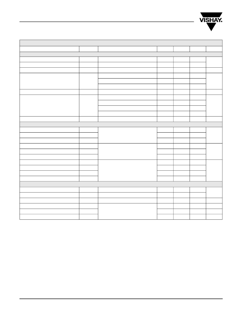
�SPECIFICATIONS� T� J� =� 25� °C,� unless� otherwise� noted�
�Parameter�
�Symbol�
�Test� Conditions�
�Min�
�Typ� a�
�Max�
�Unit�
�Static�
�Drain-Source� Breakdown� Voltage�
�Gate� Threshold� Voltage�
�Gate-Body� Leakage�
�V� (BR)DSS�
�V� GS(th)�
�I� GSS�
�V� GS� =� 0� V,� I� D� =� 250� μA�
�V� DS� =� V� GS� ,� I� D� =� 250� μA�
�V� DS� =� 0� V,� V� GS� =� ±� 20� V�
�150�
�2�
�±� 100�
�V�
�nA�
�V� DS� =� 120� V,� V� GS� =� 0� V�
�1�
�Zero� Gate� Voltage� Drain� Current�
�I� DSS�
�V� DS� =� 120� V,� V� GS� =� 0� V,� T� J� =� 125� °C�
�50�
�μA�
�V� DS� =� 120� V,� V� GS� =� 0� V,� T� J� =� 175� °C�
�250�
�On-State� Drain� Current� b�
�I� D(on)�
�V� DS� =� 5� V,� V� GS� =� 10� V�
�V� GS� =� 10� V,� I� D� =� 15� A�
�25�
�0.077�
�0.095�
�A�
�Drain-Source� On-State� Resistance� b�
�r� DS(on)�
�V� GS� =� 10� V,� I� D� =� 15� A,� T� J� =� 125� °C�
�V� GS� =� 10� V,� I� D� =� 15� A,� T� J� =� 175� °C�
�V� GS� =� 6� V,� I� D� =� 10� A�
�0.081�
�0.190�
�0.250�
�0.100�
�Ω�
�Forward�
�Transconductance� b�
�g� fs�
�V� DS� =� 15� V,� I� D� =� 15� A�
�25�
�S�
�Dynamic� a�
�Input� Capacitance�
�C� iss�
�900�
�Gate-Drain� Charge�
�Output� Capacitance�
�Reverse� Transfer� Capacitance�
�Total� Gate� Charge� c�
�Gate-Source� Charge� c�
�c�
�Turn-On� Delay� Time� c�
�C� oss�
�C� rss�
�Q� g�
�Q� gs�
�Q� gd�
�t� d(on)�
�V� GS� =� 0� V,� V� DS� =� 25� V,� f� =� 1� MHz�
�V� DS� =� 75� V,� V� GS� =� 10� V,� I� D� =� 15� A�
�115�
�70�
�20�
�5.5�
�7�
�8�
�25�
�12�
�pF�
�nC�
�Rise� Time� c�
�Turn-Off� Delay� Time� c�
�Fall� Time� c�
�t� r�
�t� d(off)�
�t� f�
�V� DD� =� 75� V,� R� L� =� 5� Ω�
�I� D� ?� 15� A,� V� GEN� =� 10� V,� R� G� =� 2.5� Ω�
�35�
�17�
�30�
�55�
�25�
�45�
�ns�
�Source-Drain� Diode� Ratings� and� Characteristics� (T� C� =� 25� °C)� b�
�Continuous� Current�
�Pulsed� Current�
�I� S�
�I� SM�
�15�
�25�
�A�
�Forward� Voltage� a�
�Reverse� Recovery� Time�
�Peak� Reverse� Recovery� Current�
�Reverse� Recovery� Charge�
�V� SD�
�t� rr�
�I� RM(REC)�
�Q� rr�
�I� F� =� 15� A,� V� GS� =� 0� V�
�I� F� =� 15� A,� di/dt� =� 100� A/μs�
�0.9�
�55�
�5�
�0.13�
�1.5�
�85�
�8�
�0.34�
�V�
�ns�
�A�
�μC�
�Notes:�
�a.� Pulse� test;� pulse� width� ≤� 300� μs,� duty� cycle� ≤� 2� %�
�b.� Guaranteed� by� design,� not� subject� to� production� testing.�
�c.� Independent� of� operating� temperature.�
�Stresses� beyond� those� listed� under� “Absolute� Maximum� Ratings”� may� cause� permanent� damage� to� the� device.� These� are� stress� ratings� only,� and� functional� operation�
�of� the� device� at� these� or� any� other� conditions� beyond� those� indicated� in� the� operational� sections� of� the� specifications� is� not� implied.� Exposure� to� absolute� maximum�
�rating� conditions� for� extended� periods� may� affect� device� reliability.�
�www.vishay.com�
�2�
�Document� Number:� 71642�
�S-71662-Rev.� B,� 06-Aug-07�
�发布紧急采购,3分钟左右您将得到回复。
相关PDF资料
SUP28N15-52-E3
MOSFET N-CH D-S 150V TO220AB
SUP40P10-43-GE3
MOSFET P-CH 100V 36A TO220AB
SUP45N03-13L-E3
MOSFET N-CH D-S 30V TO220AB
SUP60N02-4M5P-E3
MOSFET N-CH D-S 20V TO220AB
SUP60N10-16L-E3
MOSFET N-CH D-S 100V TO220AB
SUP60N10-18P-E3
MOSFET N-CH D-S 100V TO220AB
SUP65P04-15-E3
MOSFET P-CH 40V 65A TO220AB
SUP75N03-04-E3
MOSFET N-CH D-S 30V TO220AB
相关代理商/技术参数
SUP18N15-95-T1-E3
制造商:Vishay Intertechnologies 功能描述:N CHANNEL MOSFET, 150V, 18A, Transistor Polarity:N Channel, Continuous Drain Cur
SUP-200
制造商:Sunhayato 功能描述:
SUP-2400
制造商:Distributed By MCM 功能描述:DirecTV B Band Converter 制造商:MCM 功能描述:B-BAND CONVERTER
SUP28N15-52
功能描述:MOSFET 150V 28A 120W RoHS:否 制造商:STMicroelectronics 晶体管极性:N-Channel 汲极/源极击穿电压:650 V 闸/源击穿电压:25 V 漏极连续电流:130 A 电阻汲极/源极 RDS(导通):0.014 Ohms 配置:Single 最大工作温度: 安装风格:Through Hole 封装 / 箱体:Max247 封装:Tube
SUP28N15-52_07
制造商:VISHAY 制造商全称:Vishay Siliconix 功能描述:N-Channel 150-V (D-S) 175 Celsius MOSFET
SUP28N15-52-E3
功能描述:MOSFET 150V 28A 120W RoHS:否 制造商:STMicroelectronics 晶体管极性:N-Channel 汲极/源极击穿电压:650 V 闸/源击穿电压:25 V 漏极连续电流:130 A 电阻汲极/源极 RDS(导通):0.014 Ohms 配置:Single 最大工作温度: 安装风格:Through Hole 封装 / 箱体:Max247 封装:Tube
SUP31950-1
制造商:Panasonic Industrial Company 功能描述:PC BOARD
SUP33N20-60P-E3
功能描述:MOSFET 200V 33A 156W RoHS:否 制造商:STMicroelectronics 晶体管极性:N-Channel 汲极/源极击穿电压:650 V 闸/源击穿电压:25 V 漏极连续电流:130 A 电阻汲极/源极 RDS(导通):0.014 Ohms 配置:Single 最大工作温度: 安装风格:Through Hole 封装 / 箱体:Max247 封装:Tube